Discover how hardware-software co-design, custom AI chips, and AI accelerators are optimizing next-generation AI workloads for performance and efficiency.
Every serious AI system today runs into the same wall. Models keep getting bigger, training runs keep getting longer, and the electricity bill keeps climbing. General-purpose processors were never designed for this kind of work. They handle it, but at a cost that stops making sense once workloads reach production scale.
That is why hardware-software co-design has moved from a niche research topic to a strategic priority for anyone building serious AI infrastructure. Chip architects and machine learning engineers are now sitting in the same rooms, arguing about memory bandwidth and tensor operations before a single line of production code gets written. The result is a new generation of AI hardware built specifically for the workloads it will run.
The approach means developing silicon and the algorithms that run on it as a single system, not two separate problems. Instead of writing software to fit whatever chip is available, engineering teams design the chip around the specific patterns their models will execute.
For AI, that means starting with the math. Transformer models rely heavily on matrix multiplication, attention mechanisms, and sparse computation. A chip built with those operations in mind can process them far more efficiently than a general processor asked to do the same job. The software layer, meanwhile, gets compilers, kernels, and runtimes tuned to squeeze every cycle out of the underlying silicon.
Standard CPUs and even off-the-shelf GPUs were built to be flexible. They can run a database query, a video game, or a deep learning model with roughly equal willingness. That flexibility becomes the problem when you are serving billions of tokens a day.
Modern AI chips built with a narrower purpose can pack more compute per watt, more memory bandwidth per die, and more model parameters into the same physical footprint. The economics start to matter fast. A cluster running custom silicon for a specific inference workload can deliver meaningfully higher throughput than a comparable general-purpose setup, at a fraction of the operating cost.
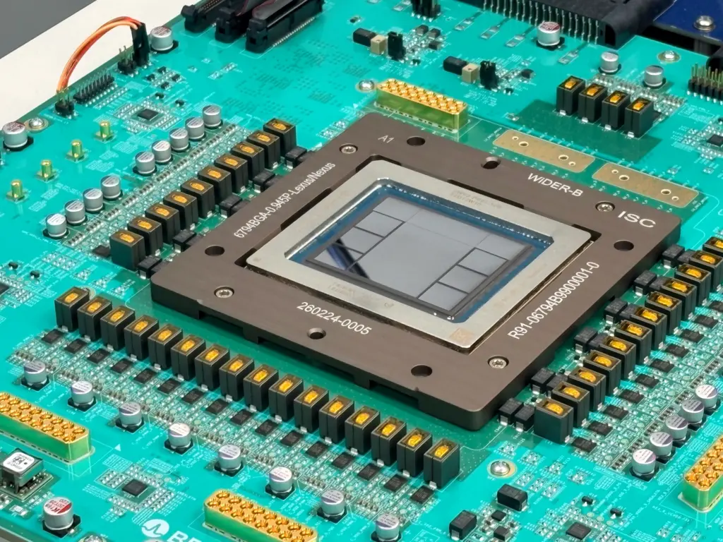
These purpose-built chips are designed around one job: running neural networks fast. They abandon the general-purpose overhead and dedicate silicon area to the operations models actually use.
Three architectural choices tend to drive the gains:
The combination is what makes purpose-built silicon feel like a different category of product, not a faster version of the same one.
Hyperscalers figured this out first. Google’s TPUs, Amazon’s Trainium and Inferentia, Microsoft’s Maia, and Meta’s MTIA all exist because renting someone else’s general-purpose chips stopped making financial sense at scale. Each of those programs represents a serious bet that purpose-built processors will outperform the alternatives for the workloads that matter most.
The pattern is spreading. AI-first startups are taping out their own accelerators. Enterprise buyers are asking cloud providers which silicon their workloads will actually run on. Chip design tools that once required a semiconductor PhD are becoming accessible to smaller teams. The barrier to building AI hardware matched to a specific model architecture keeps dropping.
For anyone planning AI infrastructure decisions over the next two years, the takeaway is straightforward. Generic compute will keep working, but it will keep getting more expensive relative to purpose-built options. Teams that understand their model architecture well enough to influence silicon choices, or partner with someone who does, will operate with a real cost advantage.
The co-design mindset also changes how AI teams organize. The old boundary between hardware people and software people is fading. Model architects need to understand memory hierarchies. Chip designers need to read model papers. That shared vocabulary is where the next round of performance gains will come from. Recruiting patterns follow. Job listings that once split neatly into firmware, systems, and applied research now blend all three, and compensation for engineers who can move fluently between abstraction layers reflects how scarce that combination still is.
It is the practice of designing chips and the software that runs on them together, as one integrated system. In AI, it means building silicon around the specific model architectures and operations it will execute, rather than adapting software to whatever general-purpose chip happens to be available.
Modern AI models perform enormous volumes of matrix math, memory movement, and parallel computation. General-purpose processors can handle these workloads, but at high cost in energy, latency, and dollars. Purpose-built silicon runs the same operations far more efficiently, which matters at production scale.
They are chips designed specifically to run neural network workloads. They dedicate silicon area to tensor operations, high-bandwidth memory, and the compute patterns that dominate modern models, delivering higher throughput per watt than general processors.
These are processors built for a specific set of AI workloads or model families rather than for broad flexibility. Examples include Google’s TPUs, Amazon’s Trainium, and Microsoft’s Maia, each designed to optimize a particular slice of training or inference.
They match silicon architecture to the actual compute patterns of the target workload. That means specialized compute units, memory placed close to processing elements, and software stacks co-designed with the hardware to eliminate the idle time and bottlenecks that hurt performance on general chips.