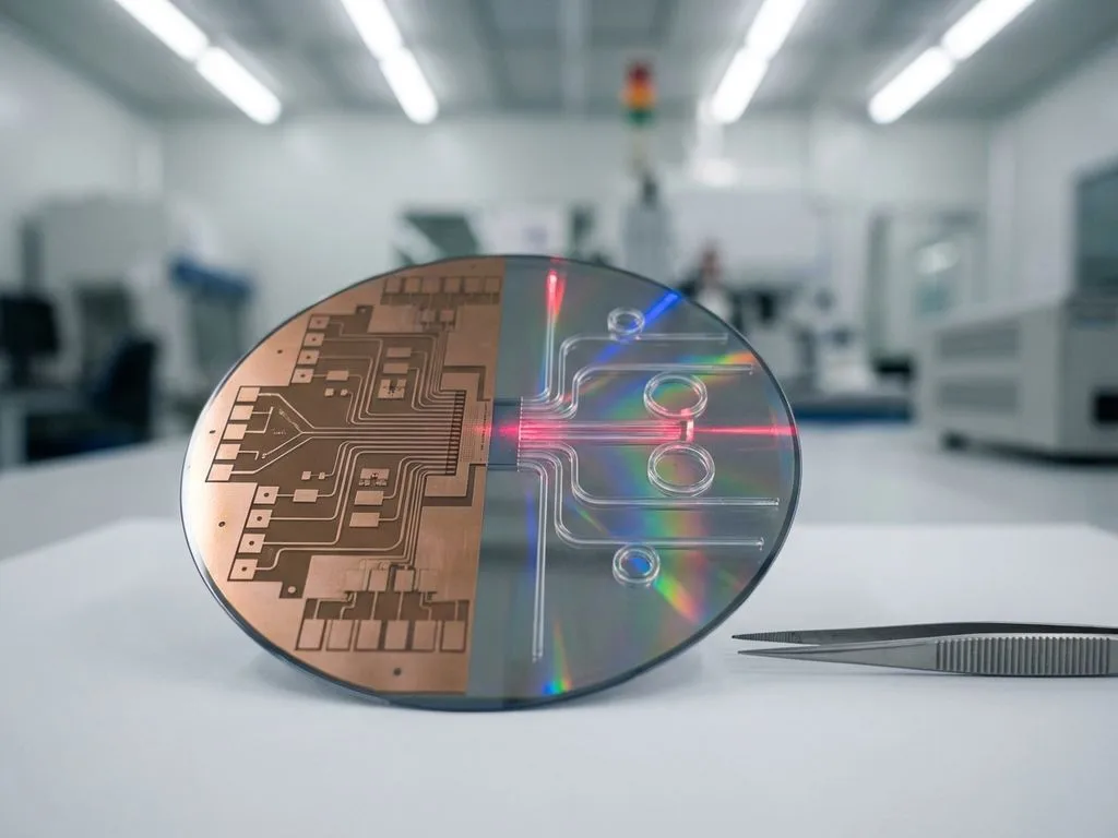
Discover how photonic chips and optical computing are solving AI hardware limitations and improving enterprise AI performance.
The AI revolution has hit a wall. Not a conceptual one-the algorithms work. The data exists. The applications are clear. The bottleneck is physical. Traditional AI chips built on silicon electronics are running into hard limits. Heat dissipation becomes a nightmare at scale. Power consumption skyrockets. Latency won’t budge. Enterprise teams are paying astronomical sums to run inference workloads, and the returns are diminishing as they throw more compute at the problem.
Enter optical chips. Instead of moving electrons through circuits, photonic chips move photons-light itself. It sounds like science fiction, but it’s happening in labs and production facilities right now. Companies are shipping AI hardware solutions based on optical computing that outperform traditional AI chips by orders of magnitude on specific workloads. For enterprises drowning in compute costs, this isn’t incremental improvement. It’s a potential game-changer.
Let’s talk about what’s really happening in AI hardware, why photonic computing matters, and why the enterprises that move early will have an advantage.
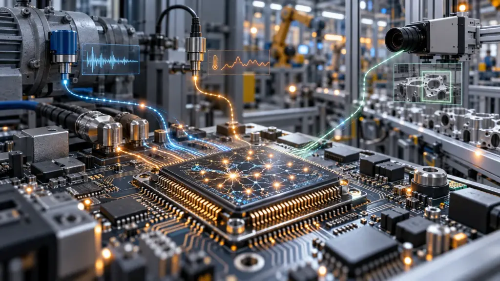
Optical chips, also called photonic chips, use light instead of electricity to process information. Traditional silicon AI chips rely on moving electrons through transistors. It’s brutally power-hungry and generates enormous heat, especially when you’re running billions of operations per second across thousands of chips. Photonic chips take a different approach: they encode information in light waves and manipulate those waves using optical components-lasers, waveguides, modulators, and detectors.
The fundamental difference is efficiency. Light travels at light speed (obviously), and photons don’t generate heat the way electrons do. When you’re processing data for enterprise AI applications-training models, running inference, processing massive datasets-those efficiency gains compound fast.
Here’s what makes optical computing technically distinct from traditional AI hardware: optical systems can theoretically achieve higher bandwidth with lower power consumption. A single optical fiber can carry vastly more information than a copper wire. Photons don’t interfere with each other the way electrons do in dense circuits. There’s no crosstalk, no electrical noise, no heat buildup forcing you to throttle performance.
Silicon photonics, the specific branch of engineering that builds photonic chips, integrates optical components onto silicon wafers. That’s huge. It means existing semiconductor manufacturing infrastructure can be adapted, costs can eventually scale down, and integration with traditional electronics becomes practical. You’re not reinventing the entire supply chain; you’re evolving it.
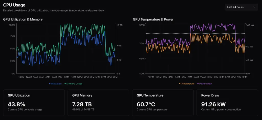
Enterprise teams building AI hardware infrastructure face brutal economics. A large language model inference setup requires multiple GPUs per request. Hyperscalers are throwing thousands of chips at the problem just to keep latency reasonable. Power bills are astronomical. Cooling requirements demand physical infrastructure that traditional data centers can barely support. And the problem is getting worse, not better.
High-performance computing has always been power-limited. You can only pack so many transistors into a space before heat kills you. Optical systems sidestep this constraint entirely. Photons carry data without heating up the substrate. You can achieve dramatically higher computational density without the cooling nightmare.
For specific workloads-particularly matrix multiplications, which are at the heart of deep learning-optical chips show stunning advantages. Research prototypes have demonstrated 100x improvements in energy efficiency for certain AI tasks compared to traditional AI chips. Even accounting for practical inefficiencies, achievable gains are in the 10x to 50x range. That transforms the economics of enterprise AI overnight.
Consider a mid-sized enterprise running continuous inference for customer-facing AI applications. With traditional GPU-based AI hardware, they’re spending millions annually on electricity alone. With photonic chips, that cost shrinks to a fraction. The payback period goes from years to months. Suddenly, AI applications that were economically marginal become profitable.
The move from traditional AI hardware to optical computing isn’t just a tech upgrade. It’s strategic.
First, there’s the efficiency story. High-performance computing via photonic chips means enterprises can run more sophisticated models, process more data, and serve more users without proportional increases in energy consumption. For companies operating at scale-financial institutions running fraud detection, e-commerce platforms personalizing search, insurance firms pricing risk-this efficiency gain is genuinely transformative.
Second, there’s capacity. Data center constraints are real. Adding GPU capacity requires physical space, cooling infrastructure, power delivery, and capital investment. With optical chips requiring a fraction of the power and cooling, enterprises can expand computational capacity without building new facilities.
Third, there’s competitive positioning. Early adopters of photonic chips in AI workloads will have cost and performance advantages over competitors still relying on traditional AI chips. That’s not permanent-technology diffuses-but the window where you get that edge lasts years, not months.
Fourth, there’s the emerging regulatory angle. Energy consumption is becoming a regulatory concern in many jurisdictions. AI workloads consuming enormous amounts of electricity are drawing scrutiny. Optical computing architectures that dramatically reduce power requirements align with sustainability goals and help enterprises stay ahead of regulatory trends.
Photonic chips won’t replace traditional AI chips everywhere. They’re phenomenal for specific tasks but not universal. Training massive models still benefits from GPU parallelism. Small inference tasks don’t benefit from optical systems’ advantages. But for large-scale inference, data center-level AI processing, and energy-constrained scenarios, optical computing is becoming genuinely competitive.
The engineering challenges are real but solvable. Integration between optical and electrical components is the big one. Most systems will be hybrid-using photonic chips for computation-heavy sections and traditional electronics for control logic. That hybrid approach is already being built and tested.
Silicon photonics manufacturing is advancing rapidly. Companies that historically focused on optical telecom infrastructure are now targeting AI workloads. The cost curve is steep. Early photonic chips are expensive because volumes are low. But once demand scales, manufacturing costs follow predictable trajectories downward. We’re in the early-adoption phase now.
AI hardware evolution isn’t slowing down. If anything, the pressure intensifies. Training models grow more computationally expensive each year. Inference workloads are proliferating across every industry. Power constraints are tightening. Traditional AI chips can’t keep up with the demand curve.
Optical chips and photonic computing represent a meaningful step forward. They’re not a magic bullet-no single technology ever is-but they’re a legitimate breakthrough that changes the economics and physics of AI at scale.
For enterprises building serious AI infrastructure, paying attention to optical computing isn’t optional anymore. It’s about understanding where the technology is heading, evaluating pilot projects, and positioning yourself to adopt when the time is right. The enterprises that move thoughtfully now will have structural advantages in the next 3-5 years as photonic chips scale from niche to mainstream.
Optical chips improve AI performance by using photons instead of electrons to process data, dramatically reducing power consumption and heat generation. Light-based computation enables higher bandwidth with lower latency for certain workloads. Photonic chips excel at matrix multiplications central to deep learning, achieving 10x to 50x improvements in energy efficiency compared to traditional electronic AI chips. This means enterprises can run larger models, process more data, and serve more inference requests without proportional increases in power consumption or infrastructure investment.
Traditional computing uses electrons flowing through silicon transistors to represent and process data. Optical computing uses photons encoded in light waves, routed through optical components like waveguides and modulators. The key difference: electrons generate heat and face crosstalk in dense circuits, while photons travel without heating and don’t interfere with each other. Optical computing achieves higher data density and energy efficiency but requires specialized integration with traditional electronics. Most practical systems will be hybrid, leveraging both for different functions.
Photonic chips are used for high-bandwidth, energy-intensive computing tasks. In AI, they excel at inference workloads requiring massive matrix multiplications-large language model serving, computer vision processing, recommendation engines at scale. Beyond AI, photonic chips are deployed in telecommunications, data center interconnects, and high-performance computing clusters where bandwidth and power efficiency are critical. They’re particularly valuable where traditional AI hardware would require excessive cooling and power delivery infrastructure.
AI hardware determines whether enterprise AI applications are economically viable and operationally practical. Poorly optimized AI hardware leads to crushing power bills, infrastructure constraints, and latency that makes real-time applications impossible. Efficient AI hardware like photonic chips reduces computational costs, frees up data center capacity, and enables enterprises to run sophisticated models at scale. For companies deploying AI across multiple applications, AI hardware efficiency directly impacts ROI, competitive positioning, and the breadth of AI initiatives they can undertake.
Optical chips reduce energy consumption because photons don’t generate the heat that electrons do in traditional circuits. Photonic computing achieves computational density without the power-hungry cooling requirements that plague high-performance computing on silicon. Light signals travel without electrical resistance losses. Optical waveguides don’t experience crosstalk, eliminating inefficiencies in dense circuits. The result: processing equivalent computational workloads with 10-50x less power consumption. For data centers running continuous inference, this translates directly to lower electricity costs and reduced environmental impact.